|
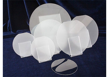
Product Details:
|
| Material: | GaN | Type: | GaN-FS-10, GaN-FS-15 |
|---|---|---|---|
| Orientation: | C-axis(0001) ± 0.5° | TTV: | ≤15 µm |
| BOW: | ≤20 µm | Carrier Concentration: | >5x10¹⁷/cm3 |
| Typical Thickness (mm): | N-type, Semi-Insulating | Resistivity(@300K): | < 0.5 Ω•cm, >106 Ω•cm |
| Usable Surface Area: | > 90% |
With wide direct bandgap(3.4 eV), strong atomic bonds, high thermal conductivity and excellent radiation resistance, GaN is not only short-wave-length optoelectronic material, but also a well alternative material for high temperature semiconductor devices. Based on the stable physical and chemical properties, GaN is suitable for LED applications (blue, green, UV-light), ultraviolet detectors and optoelectronic high-power and high-frequency devices.
| Specification | ||
| Type | GaN-FS-10 | GaN-FS-15 |
| Size | 10.0mm×10.5mm | 14.0mm×15.0mm |
| Thickness |
Rank 300, Rank 350, Rank 400 |
300 ± 25 µm, 350 ± 25 µm, 400 ± 25 µm |
| Orientation | C-axis(0001) ± 0.5° | |
| TTV | ≤15 µm | |
| BOW | ≤20 µm | |
| Carrier Concentration | >5x10¹⁷/cm3 | / |
| Conduction Type | N-type | Semi-Insulating |
| Resistivity(@300K) | < 0.5 Ω•cm | >106 Ω•cm |
| Dislocation Density | Less than 5x106 cm-2 | |
| Useable Surface Area | > 90% | |
| Polishing |
Front Surface: Ra < 0.2nm. Epi-ready polished Back Surface: Fine ground |
|
| Package | Packaged in a class 100 clean room environment, in single wafer containers, under a nitrogen atmosphere. | |
Contact Person: JACK HAN
Tel: 86-18655618388